Silicon IP Products
Quantum Leap Solutions offers an extensive portfolio of silicon proven digital and analog IP across many process platforms. IP is available Off the Shelf or can be ported or customized to your application requirements.
- Best in class Silicon Proven IP and ASIC solutions
- IP customized for your application & market
- Specifications, process offerings, and deliveries
- Flexible IP and ASIC engagement models:
- IP Licensing and services
- Turnkey ASICs – specializing in wireless & mixed signal ASICs
- Standard Product to ASIC conversion services to reduce cost & protect your IP
- Turnkey manufacturing services for packaging, assembly and test
- View our Partners' offerings in our QLS Partner Portfolio
IP Partner Offerings

Agile Analog IP
Agile Analog is transforming the world of analog IP, with our innovative solutions and subsystems for Data Conversion, Power Management, IC Monitoring, Security and Always-On IP. Our customizable analog IP products do not have a pre-determined set of features and specifications. You specify the IP you want, to include all the features you need. We generate the IP you have specified: fully tested, fully documented, bug-free and fab-ready.
Using our configurable, multi-process analog IP technology you can:
- Work with any foundry, on any process and node
- Optimize your analog designs, simplify your SoCs
- Reduce the cost of custom development
- Regain control of your analog IP design flow
- Reduce the complexity of analog IP integration
- Bring analog on chip as you need it
Contact Us For Information

QuickLogic
QuickLogic, a trusted partner of Quantum Leap Solutions, brings over 35 years of expertise in FPGA technology. Headquartered in San Jose, CA, and ISO-9001 certified, QuickLogic is a NASDAQ-listed company (QUIK) known for its innovative programmable logic solutions.
Key Offerings:
- eFPGA IP: QuickLogic's embedded FPGA Intellectual Property (eFPGA IP) enhances integration, reduces latency, and lowers power consumption compared to traditional FPGAs. It supports a wide range of process nodes from 12nm to 250nm, making it suitable for various applications, including commercial, automotive, and radiation-hardened environments.
- Design Services: QuickLogic offers comprehensive design services to help customers achieve efficient, reliable, and scalable reprogrammable logic architectures. Their open-source tools and flexible solutions ensure fast time-to-market and easy integration with standard ASIC tool flows.
- Device Storefront: QuickLogic provides a storefront for FPGAs, chiplets, and more, catering to diverse customer needs.
Market Applications:
QuickLogic's solutions are widely adopted in various markets, including aerospace and defense, industrial automation, automotive, data centers, and wireless communication. Their eFPGA technology is particularly beneficial for applications requiring efficient calculation, precise timing, security, and size, weight, power, and cost reduction (SWAP-C).
Recognition:
QuickLogic has been honored with multiple awards, including BAE Systems' 'Partner 2 Win' Supplier of the Year award and the 'FAST LabsTM Technology Innovation Partner Of The Year' award, highlighting their dedication to delivering state-of-the-art embedded FPGA Hard IP capability to the Defense Industrial Base.
Innovative Solutions:
QuickLogic's FPGA-based solutions offer flexibility, adaptability, and built-in security features. Their technology enables continuous reprogramming to comply with updated security standards, making them a pivotal tool in the defense against cyberattacks.
Future Vision:
QuickLogic is committed to advancing programmable logic solutions with their chiplet vision, supporting new process nodes and enabling seamless integration with other chiplets based on application needs.


Contact Us For Information

Silicon Creations
Silicon Creations supplies high performance IP from a broad portfolio of wide-range PLLs, High-Speed IOs and SerDes that is silicon proven and in mass production in many wafer fabs and in process nodes ranging from 3nm to 180nm, trending toward the angstrom era. These highly-programmable products, together with a solid development flow and industry-leading support has led to a growing list of repeat customers who voice their satisfaction with us.
Our comprehensive design and verification flow backed by detailed models calibrated to silicon results assures you that any customizations we make to our IP for our customers are low risk. We use our test lab, equipped with measurement equipment automated with Matlab to generate comprehensive reports on the functionality of new IP.
Key Offerings:
- A variety of versatile ring PLLs programmable for very-low power and for low jitter, suitable for battery operated devices and applications including system clocking, precision AFE and ADC timing, SerDes reference clocks and DDR interfaces.
- Fully integrated LC PLLs with ultra low jitter approaching that of single chip products.
- Analog glue functions such as differential buffers and multiplexers for low jitter clock distribution, Power on Reset (PoR) and Bandgap Circuits
- Free running oscillators with low power and excellent precision over PVT.
- Crystal oscillators providing reference clock to the SoC from off-chip crystal or MEMS resonators.
- SerDes analog layers (PMAs) with speeds from 100Mbps to 33Gbps with ultra-low latency and fast burst mode.
- Bi-directional LVDS interfaces and video display interfaces.
- Entire IP portfolio available for automotive use through Automotive Documentation generation driven by Automotive Functional Safety trained engineering team driven by ISO 26262 and ISO 9001 quality assurance standards
In addition to this wide portfolio of proven IP, Silicon Creations is happy to discuss your custom timing or interface application and can develop a semi-custom solution for you based on silicon proven blocks. By combining creative and novel design techniques with proven circuit architectures and verification methodologies, we deliver leading performance with low risk while maintaining highly competitive pricing and delivery times. Please review the list of our products on Design & Reuse and ChipEstimate .
Contact Us For Information

Certus Semiconductor
Certus Semiconductor is a Unique IO & ESD Solution Company
We have assembled several of the world’s foremost experts in IO and ESD design to offer our clients the ability to affordably tailor their IO libraries into the optimal fit for their products. We work directly with you - that means we will meet with your architects, circuit & layout designers and reliability engineers to ensure that our IO and ESD solutions provide the most efficient and competitive solutions for your market space.
Digital I/O
- Certus Semiconductor’s digital I/O solutions are capable of meeting many GPIO/ODIO standards including I2C, I3C, SPI, JECDEC CMOS, eMMC, LPDDR, SMBUS, DDC/DEC, ECEL,GTL, RGMII2, SPDIF and many more.
Foundries
- Certus Semiconductor has silicon-proven libraries in TSMC, GlobalFoundries, and Samsung processes. These libraries can be licensed off-the-shelf or can be customized for your specific application, and are available as full libraries or on a cell-by-cell basis. We have experience consulting in Intel, TowerJazz, DongBu HiTek, UMC, pSemi, Silanna, Lfoundry, Silterra, TSI, XFab, and Vanguard processes.
Design Services
Certus Semiconductor offers the following design services:
- RF/Analog Circuit Characterization and Design
- Liberty Timing Modeling
- IBIS Models for I/O’s
- Custom Standard Cell Libraries
- I/O Library/Padring Integrated Oscillators, Voltage Regulators and PLL’s
Contact Us For Information

Alphacore
High performance data converter IP silicon proven on TSMC, GlobalFoundries and Trusted Foundries. 5GS/s, 10GS/s and 20GS/s ADC and DAC architectures. Customizable to your end applications. Suitable for sensing, automotive LiDar and Radar, satellite communications, defense and aerospace applications. Radiation hardened options available as well.
Our focus areas are:
- RF IP including ADC, DAC and LNA, PA and more
- Aerospace/Defense and Government IP and ASICs
- LIDAR, RADAR
- Automotive Applications
- Replacement of obsolete and EOL analog / RF components
- ASIC and Other Services, and Emerging Technologies
Data Converter Architectures
- Delta-Sigma
- Consumer, IOT, Wearables
- High Resolution, ultra low power
- Low power up to 16 bit and 1MS/s
- Pipelined
- Consumer, WiFi, Lidar
- High Resolution, High Dynamic Range, Moderate power
- Low power up to 14 bits and 1GS/s
- Hybrid SAR
- Sat Comms, 5G, Automotive, Lidar, Exotic Compute
- Highest Sample Rate, lowest power
- Low power up to 12 bits and 64GS/s
- Parallel Flash
- Sat Comms, 5G, Automotive
- Low Resolution, Ultra-High Speed
- Lowest power in the industry
- Low power up to 6-8 bits and 80GS/s
- Analog blocks
- LDO, Bandgap, Comparators, Regulators
Contact Us For Information
IP Type Offered by QLS Partners

Design IP
- ADC, DAC - 1MS/s to 20GS/s (radiation hardened options)
- RF and AFE subsytems
- NOC (Custom Coherent and Non-Coherent Network on Chip)
Contact Us For Information

RFIC and Wireless ASICs
IP / macro solutions for your wireless designs
- ADC and DACs to support Lidar, Radar, 5G and SatComm applications (up to 20GS/s)
- ADCs and DACs to support Industrial IoT, WiFi and BLE applications
- Automotive Fusa and ASIL-B, ASIL-D design support
- RF and mmwave macro and design expertise
- MIMO beamforming
- PCIe gen 3/4/5
- RFICs and mixed signal ASICs
Contact Us For Information

Automotive Sensors
Automotive IP from our partners
Areas of expertise:- Lidar, Radar, Sensors, ADAS
- ADC/DAC up to 20GB/s sampling (customizable)
- ASIL-B, ASIL-D support
- 25GE, Automotive Ethernet
- C-PHY, D-PHY, A-PHY
- RFIC and Mixed Signal ASICs
Contact Us For Information
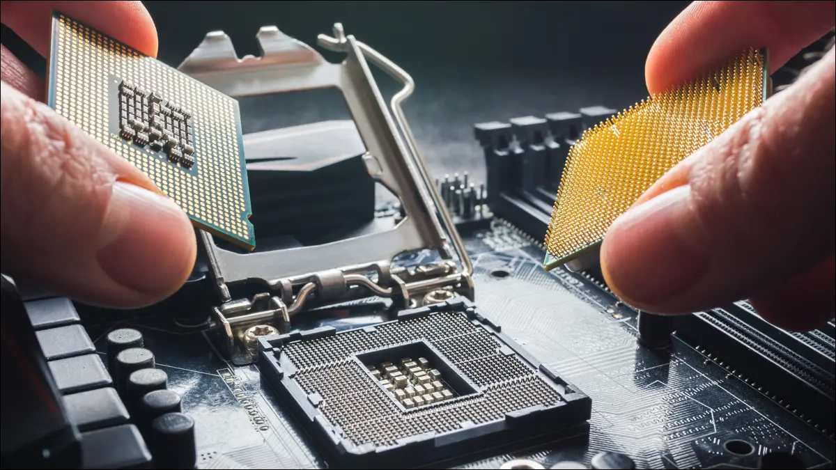
Chiplets
Chiplet technology is a different way of integrating multiple dies in a package or system. There are several approaches to chiplets. The basic idea is that you have a menu of modular chips, or chiplets, in a library. Then, you assemble chiplets in a package and connect them using a die-to-die interconnect scheme. In theory, the chiplet approach is a fast and less expensive way to assemble various types of third-party chips, such as I/Os, memory and processor cores, in a package.
With an SoC, a chip might incorporate a CPU, plus an additional 100 IP blocks on the same chip. That design is then scaled by moving to the next node, which is an expensive process. With a chiplet model, those 100 IP blocks are hardened into smaller dies or chiplets. In theory, you would have a large catalog of chiplets from various IC vendors. Then, you can mix-and-match them to build a system. Chiplets could be made at different process nodes and re-used in different designs.
Contact Us For Information